Hi Community!
A counter is a circuit sequential built from latches and logic gates capable of storing and counting impulses (often related to a clock signal), which receives at the input intended for this purpose, likewise it also acts as a divider of frequency.
Normally, the computation is done in binary code, which often it will be the natural binary or the natural BCD (tens counter). An electronic clock is a clock on the that the time base is electronic or electromechanical and the frequency division. It is a digital element that works based on logical states, with which it indicates an output determined on the basis of a characteristic input data, its operational function is based on the introduction to its inputs of a number in binary code corresponding to its decimal equivalent to display on the seven pins of output set to the integrated, a series of states logic that are designed to connect to an element alphanumeric in which the entered number will be displayed at the decoder inputs.
The alphanumeric element that connects to the seven outputs of the decoder is also designed to work with logical states, is a device made with an array of LED in such a way that it shows the decimal numbers from zero to nine depending on the data received from the decoder, this element is known as display name or 7-segment alphanumeric device. The decoder is internally made up of gates. logics and their internal connections are a predefined system by the designer so that its operational function is a perfect and effective coupling with the display, observe how shown below in the manufacturer's specifications. What is expected in this simulation is the display of a counter on a 7-segment display showing a sequence of numbers from 3 to 9 and then show H and U until reach position 9.
Materials & Tools
- • 7 Segment Display
- • Mimas – Spartan 6 FPGA Development Board
- • Xilinx IDE
Counter's Clock
Up first we have the counter's clock, this clock fulfills an important function so much so that thanks to this clock it can be attached to the schematically and automatically when adding the .bin to the card this works depending on the code that was used, in this case the teacher gave us a code that for every second that happens the schematic changes, it connects with the accountant. Next, it will be presented how the counter looks in the schematic and we will explain step by step the code as it works.
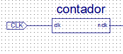
It can be seen in figure 1 that the clock is comprised of a input and an output, the CLK input goes to a specific pin on the FPGA board and the NCLK output goes to the input of the 0-9 counter circuit. Below is an explanation of the code used

The libraries that were used for the code are from the Institute of Electrical and Electronics Engineers, these comply with the IEEE format and They are necessary for logical operations.

Figure 3 shows how the ports are declared. To know which is the input and which is the output, you can Note that CLK is the input and NCLK is the output.

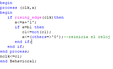
Figure 4 shows us the code that is used for the duration of time between each value of the schematic, for example when changing from one number to another, that is, from 3 to 4, there is an exact duration of 1 second, this can be changed depending on what is needed, but the standard is 1 second, it is important to give an announcement that when simulating in the same IDE it is recommended to change the value of the duration so that the results can be better appreciated, but when using The card needs to be left the way the teacher told us, because if you put a very low value, you won't see the difference on the 7-segment display and it won't give the corresponding answer. Finally, in figure 5 you can see the process as such of the clock, how it works, we can realize that the clock has a loop process inside that is repeated for a period of time and ends when it fulfills a specific function.
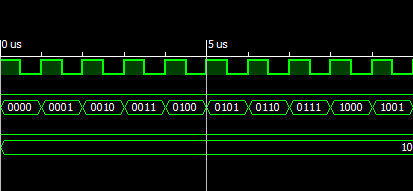
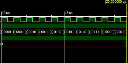
Next you can see the behavior of the counter when simulating it with Xilinx ISE. (See figure 6 and 7). If we realize the behavior looks correct, since when obtaining the pulses in the inputs of 0 and 1 the clock goes through the binary numbers 0000, 0001, 0010 and so on until reaching 1001, after this the process is repeated. same process just with the output being 1.
0-9 Counter Circuit with Flip Flops
Next we will start the complete explanation of the 0-9 counter circuit, a brief introduction to its function will be given and we will do the step by step of how this final answer was reached.
The 0-9 counter circuit with JK flip flops is a circuit whose function is to be able to count from 0 to 9 and at the end of this count repeat it again until a function is fulfilled or until the power supply is disconnected, for this it was very important adapt the clock to this circuit since the clock allowed us to change numbers second by second in an orderly manner.
Before we start making the circuit, we need to understand what a JK flip flop is.
The JK flip flop is versatile and is one of the most widely used flip-flop types. Its operation is identical to that of the S-R flip-flop in SET, RESET, and stay-on conditions. The difference is that the J-K flip-flop does not have invalid conditions like the S-R. This storage device is temporary in two states (high and low), whose main inputs, J and K, to which it owes its name, allow when activated:
J: Set, set to 1 and high level of the output. K: Reset, setting to 0 or low level of the output.
After knowing this we begin the construction of the circuit. It starts by creating the transition table which consists of the numbers 0-9 in binary:
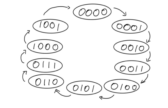
After obtaining the transition table, we proceed to make the corresponding truth table, of the current and next state and the values of J and K.
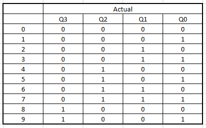
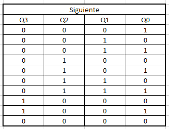
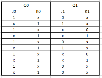
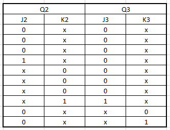
By obtaining all the truth tables, we can carry out our procedure to make the K maps step by step and thus obtain the algebraic functions for the construction of the circuit.