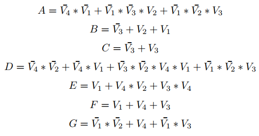
Next, all the algebraic functions obtained by the K maps are presented in order:
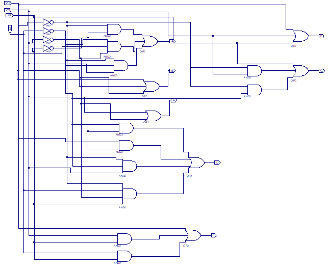
We now make the circuit with logic gates:
And its corresponding simulation is done to know if it was done correctly and it gives us all the results of the 7 segments.
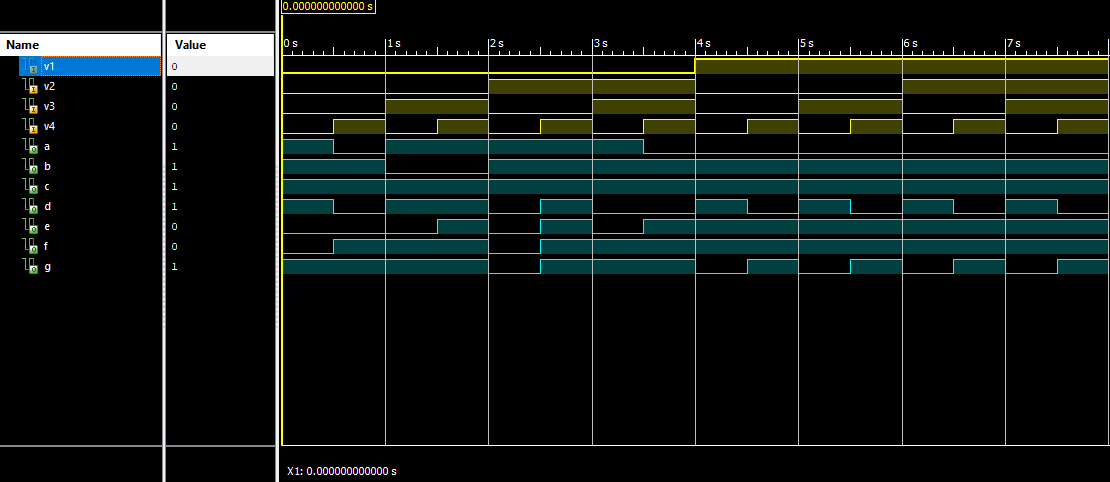
Next, the same test will be done, only by adding the clock at the input of the circuit, the difference in the values of the period will be seen.
Final Circuit & Simulation
We have already been able to see each section of our final project, how they are made up of where each element comes from and most importantly how each of these circuits works, now we will join each circuit correctly, for this it is necessary to create a schematic symbol for each one, since if the circuits are joined it will be very difficult to correctly understand the unions of these in the Xilinx, for this reason it is better to make black boxes, as was done with the clock, for each circuit and thus be able to join them at the end . First the circuits and the clock are added to our final project, after doing this the schematic symbol is created for each one (first select the schematic for which you want to create the symbol and click on "Create Schematic Symbol") , as it's shown in the following:
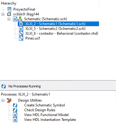
After doing this step for the two schematics and code of the clock, we go to the final schematic where all the elements will be joined and we look for the black boxes in our file section:
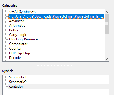
After finding our black boxes we can now output them to our final schematic and connect the inputs and outputs accordingly:
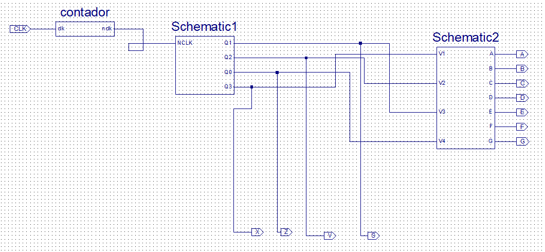
We will do its due simulation to determine that all the steps that were done were correct, the expected results would be that the 7 segments give us the numbers from 3 to 9 and then show H U H and start the count again.
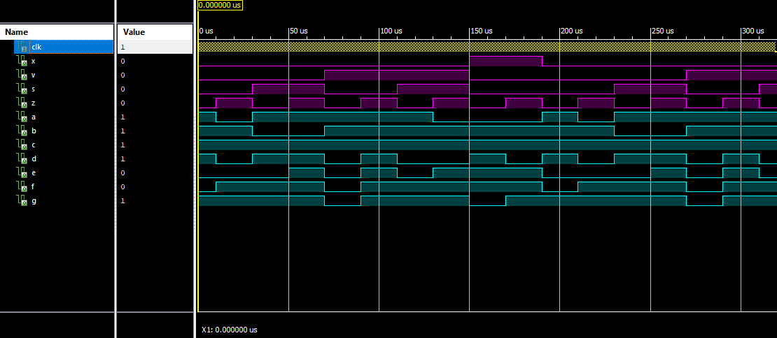
You can see the behavior of each signal is the appropriate and expected behavior, also at the end of the counter, a kind of reset is done and it starts counting again from 0 showing the number 3.
Pin configuration for the FPGA board
After making the final circuit, the pin configuration will be made to be able to insert it into the FPGA card and be able to make it work: (This part can be different dpending on which pinout you choose)


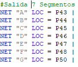
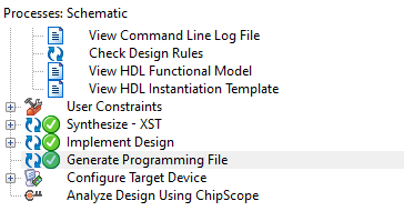
The code is done to generate the .bin and the 3 hooks must be obtained to confirm that our code is correct.
